- 您现在的位置:买卖IC网 > Sheet目录3862 > PIC18F45J11-I/ML (Microchip Technology)IC PIC MCU FLASH 32K 2V 44-QFN
2011 Microchip Technology Inc.
DS39932D-page 5
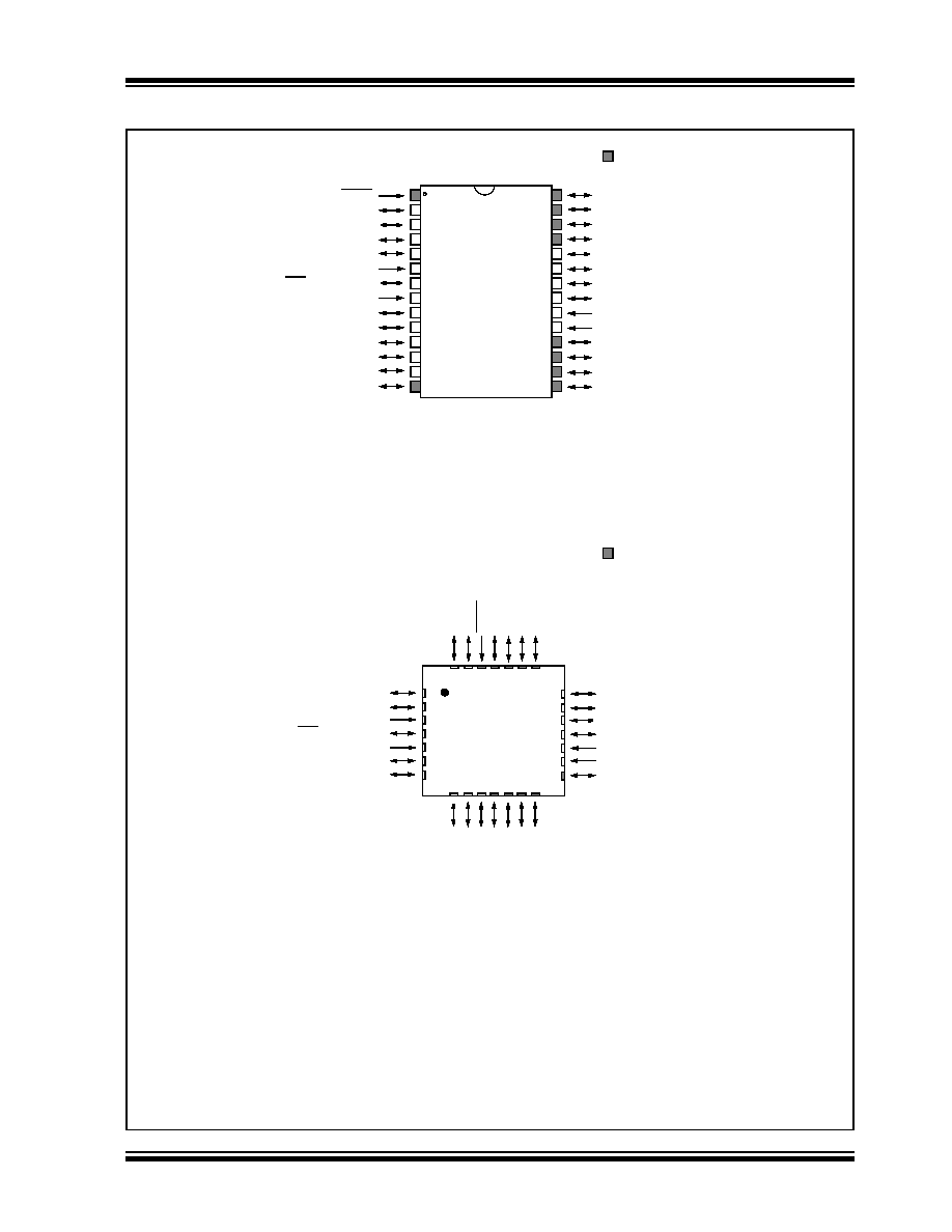
PIC18F46J11 FAMILY
Pin Diagrams
P
IC18F
2X
J1
1
10
11
2
3
4
5
6
1
8
7
9
12
13
14
15
16
17
18
19
20
23
24
25
26
27
28
22
21
MCLR
RA0/AN0/C1INA/ULPWU/RP0
RA1/AN1/C2INA/RP1
RA2/AN2/VREF-/CVREF/C2INB
RA3/AN3/VREF+/C1INB
VDDCORE/VCAP(2)
RA5/AN4/SS1/HLVDIN/RP2
VSS
OSC1/CLKI/RA7
OSC2/CLKO/RA6
RC0/T1OSO/T1CKI/RP11
RC1/T1OSI/RP12
RC2/AN11/CTPLS/RP13
RC3/SCK1/SCL1/RP14
RB7/KBI3/PGD/RP10
RB6/KBI2/PGC/RP9
RB5/KBI1/RP8
RB4/KBI0/RP7
RB3/AN9/CTED2/RP6
RB2/AN8/CTED1/REFO/RP5
RB1/AN10/RTCC/RP4
RB0/AN12/INT0/RP3
VDD
VSS
RC7/RX1/DT1/RP18
RC6/TX1/CK1/RP17
RC5/SDO1/RP16
RC4/SDI1/SDA1/RP15
28-Pin SPDIP/SOIC/SSOP(1)
Legend:
RPn
represents remappable pins.
Note
1:
Some input and output functions are routed through the Peripheral Pin Select (PPS) module and can be
dynamically assigned to any of the RPn pins. For a list of the input and output functions, see Table 10-13
and Table 10-14, respectively. For details on configuring the PPS module, see Section 10.7 “Peripheral
.
2:
3:
For the QFN package, it is recommended that the bottom pad be connected to VSS.
28-Pin QFN(1,3)
1011
2
3
6
1
18
19
20
21
22
12 13 14
15
8
7
16
17
23
24
25
26
27
28
9
PIC18F2XJ11
RC0
/T
1
O
S
O/T
1CK
I/
RP1
1
5
4
RB
7
/KBI
3/
PG
D/
RP1
0
RB
6
/KBI
2/
PG
C/
RP9
RB
5
/KBI
1/
RP
8
RB
4
/KBI
0/
RP
7
RB3/AN9/CTED2/RP6
RB2/AN8/CTED1/REFO/RP5
RB1/AN10/RTCC/RP4
RB0/AN12/INT0/RP3
VDD
VSS
RC7/RX1/DT1/RP18
RC6
/T
X
1
/CK
1/
RP1
7
RC5
/S
DO
1/
RP1
6
RC4
/SDA1
RP1
5
MC
LR
RA0
/A
N
0
/C1
IN
A/UL
PWU/
RP0
RA
1
/AN1
/C
2I
N
A/
RP1
RA2/AN2/VREF-/CVREF/C2INB
RA3/AN3/VREF+/C1INB
VDDCORE/VCAP(2)
RA5/AN4/SS1/HLVDIN/RP2
VSS
OSC1/CLKI/RA7
OSC2/CLKO/RA6
RC1
/T
1O
SI/
RP1
2
RC2
/AN1
1/
CT
PL
S/
RP1
3
RC3
\SCK1
\S
C
L
1\
RP1
4
= Pins are up to 5.5V tolerant
发布紧急采购,3分钟左右您将得到回复。
相关PDF资料
SFW15R-2STE1
SFW15R-2STE1-FFC/FPC CONN
PIC18F26J11-I/ML
IC PIC MCU FLASH 64K 2V 28-QFN
PIC18F46K20-E/ML
IC PIC MCU FLASH 32KX16 44QFN
PIC24FJ64GA002-I/SO
IC PIC MCU FLASH 64KB 28SOIC
PIC16C711-04/P
IC MCU OTP 1KX14 A/D 18DIP
PIC18LF26K22-I/SP
IC PIC MCU 64KB FLASH 28SPDIP
PIC18F25K80-I/SP
MCU PIC 32KB FLASH 28SDIP
DSPIC33FJ12MC201-I/SS
IC DSPIC MCU/DSP 12K 20SSOP
相关代理商/技术参数
PIC18F45J11-I/PT
功能描述:8位微控制器 -MCU 32KB Flash 4KBRAM 12MIPS nanoWatt RoHS:否 制造商:Silicon Labs 核心:8051 处理器系列:C8051F39x 数据总线宽度:8 bit 最大时钟频率:50 MHz 程序存储器大小:16 KB 数据 RAM 大小:1 KB 片上 ADC:Yes 工作电源电压:1.8 V to 3.6 V 工作温度范围:- 40 C to + 105 C 封装 / 箱体:QFN-20 安装风格:SMD/SMT
PIC18F45J11T-I/ML
功能描述:8位微控制器 -MCU 32KB Flash 4KBRAM 12MIPS nanoWatt RoHS:否 制造商:Silicon Labs 核心:8051 处理器系列:C8051F39x 数据总线宽度:8 bit 最大时钟频率:50 MHz 程序存储器大小:16 KB 数据 RAM 大小:1 KB 片上 ADC:Yes 工作电源电压:1.8 V to 3.6 V 工作温度范围:- 40 C to + 105 C 封装 / 箱体:QFN-20 安装风格:SMD/SMT
PIC18F45J11T-I/PT
功能描述:8位微控制器 -MCU 32KB Flash 4KBRAM 12MIPS nanoWatt RoHS:否 制造商:Silicon Labs 核心:8051 处理器系列:C8051F39x 数据总线宽度:8 bit 最大时钟频率:50 MHz 程序存储器大小:16 KB 数据 RAM 大小:1 KB 片上 ADC:Yes 工作电源电压:1.8 V to 3.6 V 工作温度范围:- 40 C to + 105 C 封装 / 箱体:QFN-20 安装风格:SMD/SMT
PIC18F45J50-I/ML
功能描述:8位微控制器 -MCU Full Spd USB 32KB 4KBRAM nanoWatt RoHS:否 制造商:Silicon Labs 核心:8051 处理器系列:C8051F39x 数据总线宽度:8 bit 最大时钟频率:50 MHz 程序存储器大小:16 KB 数据 RAM 大小:1 KB 片上 ADC:Yes 工作电源电压:1.8 V to 3.6 V 工作温度范围:- 40 C to + 105 C 封装 / 箱体:QFN-20 安装风格:SMD/SMT
PIC18F45J50-I/PT
功能描述:8位微控制器 -MCU Full Spd USB 32KB 4KBRAM nanoWatt
RoHS:否 制造商:Silicon Labs 核心:8051 处理器系列:C8051F39x 数据总线宽度:8 bit 最大时钟频率:50 MHz 程序存储器大小:16 KB 数据 RAM 大小:1 KB 片上 ADC:Yes 工作电源电压:1.8 V to 3.6 V 工作温度范围:- 40 C to + 105 C 封装 / 箱体:QFN-20 安装风格:SMD/SMT
PIC18F45J50T-I/ML
功能描述:8位微控制器 -MCU Full Spd USB 32KB 4KBRAM nanoWatt RoHS:否 制造商:Silicon Labs 核心:8051 处理器系列:C8051F39x 数据总线宽度:8 bit 最大时钟频率:50 MHz 程序存储器大小:16 KB 数据 RAM 大小:1 KB 片上 ADC:Yes 工作电源电压:1.8 V to 3.6 V 工作温度范围:- 40 C to + 105 C 封装 / 箱体:QFN-20 安装风格:SMD/SMT
PIC18F45J50T-I/PT
功能描述:8位微控制器 -MCU Full Spd USB 32KB 4KBRAM nanoWatt RoHS:否 制造商:Silicon Labs 核心:8051 处理器系列:C8051F39x 数据总线宽度:8 bit 最大时钟频率:50 MHz 程序存储器大小:16 KB 数据 RAM 大小:1 KB 片上 ADC:Yes 工作电源电压:1.8 V to 3.6 V 工作温度范围:- 40 C to + 105 C 封装 / 箱体:QFN-20 安装风格:SMD/SMT
PIC18F45K20-E/ML
功能描述:8位微控制器 -MCU 32KB Flash 1536B RAM 25 I/O 8B RoHS:否 制造商:Silicon Labs 核心:8051 处理器系列:C8051F39x 数据总线宽度:8 bit 最大时钟频率:50 MHz 程序存储器大小:16 KB 数据 RAM 大小:1 KB 片上 ADC:Yes 工作电源电压:1.8 V to 3.6 V 工作温度范围:- 40 C to + 105 C 封装 / 箱体:QFN-20 安装风格:SMD/SMT